Big Blue Goes Copper
Copper Applications in Electronic & Communications
When both IBM and Motorola recently announced the replacement of aluminum with copper in their chip manufacturing process, the copper industry was pleased, to say the least. Due to the physical dimensions of the IC's (Integrated Circuits) actual effect on the worldwide consumption of copper is negligible. Pushing copper to the forefront of the fastest-growing industry in the world, however, may have some effects of its own.
The new CMOS (Complimentary Metal Oxide Semiconductor) manufacturing process takes advantage of copper's superior electrical and thermal conductivity over aluminum's. This allows for thinner, shorter interconnects in addition to greater resistance to electromigration.
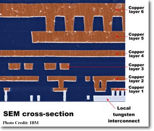 This innovative copper metallization technique produces a chip with six layers of copper circuitry with circuit line widths of 0.20 microns (See Figure). The channel length, or the distance the electrical current must travel through a transistor in integrated circuits, is where copper is making the difference.
The effective channel length of the transistors has been reduced to 0.15 microns and lower. This shorter channel length translates into faster processing speeds, and ultimately, better performance. As a result of these thinner widths and shorter lengths, up to 200 million transistors may be packed onto a single chip. Chips produced with this process can also support 2200 I/O (input/output) connections.
Until recently, there were difficulties in adapting copper to the semiconductor manufacturing process, leaving aluminum as the preferred material for more than 30 years. A technique needed to be developed to prevent interaction of the copper with the underlying silicon substrate. This new advance is a proprietary process, but is believed to involve a metallized diffusion barrier deposited before the copper layer is applied.
IBM and Motorola's chip technology will not only make computers faster, but will bring high-end computing power to portable devices such as notebook computers, PDAs (personal digital assistants), mobile phones, and range of electronic products yet to be invented. Copper's superior conductivity within the IC will permit the device to operate at a modest 1.8 volts, thus making these chips ideal for battery-operated portable electronic products due to their inherent low consumption of power.
This recent development is also a key enabling technology for semiconductor integrated circuit performance. It represents a paradigm shift needed to extend beyond the limitations presently being reached with aluminum interconnects. Samples of the first product using the copper interconnect technology is expected to introduced in the summer of 1998. Other, if not all, semiconductor manufacturers are working toward the development of similar processes needed in order to successfully compete in the future. Over time, copper is expected to be the predominant metal used in high performance integrated circuits.
While the impact of the interconnects is not expected to influence the copper consumption, the decrease in operating voltage could influence the selection of the leadframe alloy. Low voltages would inherently produce cooler chips resulting in a decreased need for high temperature resistant leadframe alloys. ![]()
Also in this Issue:
- How Do They Do That? How Copper is Made
- Traditional Pyrometallurgical Treatment of Concentrate
- How Do They Do That? In Situ Mining
- Millions of Dollars Saved With Non-Traditional Shutdown Procedures
- How Do They Do That? Bringing Copper to Market
- Big Blue Goes Copper
- How Do They Do That? Wringing Sulfuric Acid out of Sulfur Dioxide Emissions